A Fan-Tas-Tic firmware upgrade
I’ve been recently re-writing major parts of my pinball controller firmware and would like to take this opportunity to show how some parts of it work behind the scenes. This is mostly about the stuff going on in bit_rules.c.
The main idea is to use PCF8574 I2C port extenders for a majority of the in and outputs. This makes the system very flexible as multiple in- and output boards can be placed in the machine wherever they are needed. Also boards of different function can coexist on the same bus, e.g., switch inputs, solenoid outputs, servo outputs, led outputs …
Firmware
Let’s have a closer look at how the firmware deals with the GPIO expanders on 4 I2C channels simultaneously.
main()
The main function starts 3 FreeRTOS tasks, all of which loop forever.
taskDemoLED()
Right now this justs prints a welcome message to the UART and then blinks the user LED. Also it clears globalDebugEnabled after 1 second, which will make all UARTprintf() calls return immediately without printing to UART.
If any character is received over UART, debug messages are enabled again.
task_pcf_io()
This task coordinates everything in- and output related. It uses vTaskDelayUntil() to achieve a more or less accurate 1 ms cycle time.
It triggers the I2C state machine, which will carry out all pending I2C transactions in the background, using interrupts. At the same time, the 8x8 switch matrix is scanned using simple NOP delay loops.
Both actions take approximately the same amount of time (< 0.5 ms) and when both are completed, process_IO() is called, which takes care of debouncing the raw samples of all inputs and keeps track of time for pulsed outputs and quick-fire rules.
Finally a few pending one-shot I2C transactions are carried out (from the I2C command) and the cycle continues.
The I2C state machine
init variables, start first I2C job"]-->B B["I2C_PCF
get I2C result, count errors, start next job"]-->B B--"notify task_pcf_io()"-->D D--"trigger from task_pcf_io()"-->C["I2C_CUSTOM
get result of a one-shot I2C job"] C--"notify task_pcf_io()"-->D
Here’s a logic analyzer capture showing 3 of the 4 I2C channels iterating over all the 8 PCF addresses. The lowest trace shows when the I2C interrupt service routine (isr) is active.
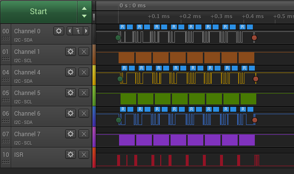
All 4 I2C channels have their own state machine. Once triggered by task_pcf_io(), each one iterates through addresses 0x20 - 0x27, which is the range where PCF8574 chips can be configured for. They read or write one byte, depending on configuration flags. If there is no I2C ACK (no PCF chip connected at this address) or another error, a counter is incremented. The whole process takes a bit less than half a millisecond, after which task_pcf_io() is notified.
Entering the command IL in the UART console shows this overview:
$ IL
  R/W[I2C_ADDR]: VAL (ERR_CNT)
  R[20]:  0 (    0)  R[20]:  0 ( 1bc5)  R[20]:  0 ( 1bc5)  R[20]:  0 ( 1bc5)
  R[21]:  0 (    0)  R[21]:  0 ( 1bc5)  R[21]:  0 ( 1bc5)  R[21]:  0 ( 1bc5)
  R[22]:  0 ( 1bc5)  R[22]:  0 ( 1bc5)  R[22]:  0 ( 1bc6)  R[22]:  0 ( 1bc6)
  R[23]:  0 ( 1bc6)  R[23]:  0 ( 1bc6)  R[23]:  0 ( 1bc6)  R[23]:  0 ( 1bc6)
  R[24]:  0 ( 1bc6)  R[24]:  0 ( 1bc6)  R[24]:  0 ( 1bc6)  R[24]:  0 ( 1bc6)
  R[25]:  0 ( 1bc6)  R[25]:  0 ( 1bc7)  R[25]:  0 ( 1bc7)  R[25]:  0 ( 1bc7)
  R[26]:  0 ( 1bc7)  R[26]:  0 ( 1bc7)  R[26]:  0 ( 1bc7)  R[26]:  0 ( 1bc7)
  R[27]:  0 ( 1bc7)  R[27]:  0 (    0)  R[27]:  0 ( 1bc7)  R[27]:  0 ( 1bc7)
R/W indicates if the channel is read or written. The number in [ ] is the I2C address. The number in ( ) is the error count in hex.
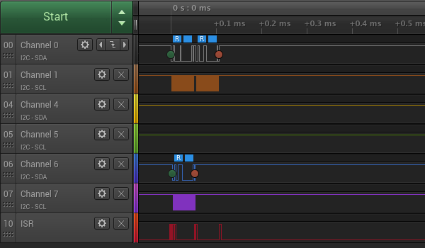
About 10 seconds after power up all error counters are evaluated. More than 9990 errors means the respective channel will be deactivated and skipped in the ISR from now on to save some processor time. In this case there were only 3 PCF chips connected. All other channels were disabled and the state machine finishes already after 0.15 ms.
The IL command in this case would show
IL
  R/W[I2C_ADDR]: VAL (ERR_CNT)
  R[20]:  0 (    0)   [20]:              [20]:              [20]:
  R[21]:  0 (    0)   [21]:              [21]:              [21]:
   [22]:              [22]:              [22]:              [22]:
   [23]:              [23]:              [23]:              [23]:
   [24]:              [24]:              [24]:              [24]:
   [25]:              [25]:              [25]:              [25]:
   [26]:              [26]:              [26]:              [26]:
   [27]:             R[27]:  0 (    0)   [27]:              [27]:
Dealing with outputs
Binary Code Modulation (BCM)
For solenoid outputs its essential to have at least a coarse control of power level. For example a solenoid shall be powered with the full 24 V, 10 A for a couple of ms to actuate but can then fall back to a fraction of this and will stay actuated. Power control has been implemented for all I2C PCF channels by binary code modulation (bcm).
For example, having a 4 bit word w = [b3, b2, b1, b0] encoding the solenoid intensity. Each bit is applied to the output for 2^i cycles, where i is the index of the bit.

If the intensity is w = 6 = 0b0110, bit b1 and b2 are high. The bcm output will be high in the blue and green regions and effectively on for 6 / 15 cycles, scaling the average power through the solenoid accordingly.
The advantage of using this method as compared to pulse width modulation (PWM) is that it scales very well for a large number of channels. It boils down to writing pre-computed words periodically to all outputs, 4 times per cycle to get 4 bits of resolution, and hence consumes little processing time, especially when the output intensity values are not changed very often.
Writing outputs
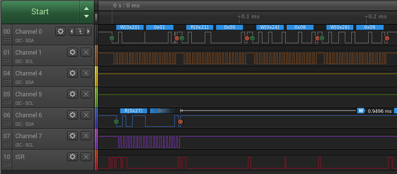
Here I use the OUT command to write various intensity values to hwIndex 64, 99, 100, 103 and 115. Each hwIndex identifies one output channel (= one bit).
$ OUT 64 1
Cmd_OUT(): i2cCh 0, i2cAdr 0x20, bit 0 = tp 0, pH 1, pL 1
$ OUT 99 1
Cmd_OUT(): i2cCh 0, i2cAdr 0x24, bit 3 = tp 0, pH 1, pL 1
$ OUT 100 2
Cmd_OUT(): i2cCh 0, i2cAdr 0x24, bit 4 = tp 0, pH 2, pL 2
$ OUT 103 4
Cmd_OUT(): i2cCh 0, i2cAdr 0x24, bit 7 = tp 0, pH 4, pL 4
$ OUT 115 1
Cmd_OUT(): i2cCh 0, i2cAdr 0x26, bit 3 = tp 0, pH 1, pL 1
Behind the scenes, the command is parsed and setPCFOutput() is called.
It adds the state of this particular output word and bit to g_outWriterList[].
First it checks if an entry for this I2C address already exists and if yes, modifies it.
If not it searches for a free slot in the array and adds a new entry.
Furthermore, set_bcm() is called, which sets the right bits in bcm_buffer()
to achieve bcm modulation of a particular intensity. The values in bcm_buffer[] are directly
written to one of the PCFs each cycle by the ISR.
An overview of the the current entries in g_outWriterList[] can be printed with the OL command.
OL
 N: [CH,I2C] PWM0 PWM1 ...
 0: [0,20]    1    0    0    0    0    0    0    0
 1: [0,24]    0    0    0    1    2    0    0    4
 2: [0,26]    0    0    0    1    0    0    0    0
Each row shows: array index: [I2C channel, I2C address].
What follows are the intensity values for all of the 8 output bits of one PCF chip.
Looking at the IL command again, it can be seen how the particular I2C addresses
are now in write mode (and there are many I2C errors as no PCF chip is connected).
IL
  R/W[I2C_ADDR]: VAL (ERR_CNT)
  W[20]:    (    0)   [20]:              [20]:              [20]:
  R[21]:  0 (    0)   [21]:              [21]:              [21]:
   [22]:              [22]:              [22]:              [22]:
   [23]:              [23]:              [23]:              [23]:
  W[24]:    ( 6ba1)   [24]:              [24]:              [24]:
   [25]:              [25]:              [25]:              [25]:
  W[26]:    ( 346b)   [26]:              [26]:              [26]:
   [27]:             R[27]:  0 (    0)   [27]:              [27]:
The write transactions are now visible on the logic analyzer as well.